InfiniBand Network
RoCE Network
Comprehensive AI Network Architecture
Immersion Cooling Network
Let's Chat
Generic Compatible 400GBASE-DR4 OSFP PAM4 1310nm 500m DOM MPO-12/APC SMF Silicon Photonics Optical Transceiver Module
US$ 630.00
Generic Compatible 800GBASE-2xDR4/DR8 OSFP PAM4 1310nm 500m DOM Dual MPO-12/APC SMF Silicon Photonics Optical Transceiver Module
US$ 729.00
Cisco QDD-400G-SR8-S Compatible 400GBASE-SR8 QSFP-DD PAM4 850nm 100m MTP/MPO FEC Optical Transceiver Module
US$ 210.00
Cisco QDD-400G-FR4-S Compatible 400GBASE-FR4 QSFP-DD PAM4 1310nm 2km DDM/DOM Duplex LC SMF Optical Transceiver Module
US$ 710.00
Cisco QDD-400G-DR4-S Compatible 400GBASE-DR4 QSFP-DD PAM4 1310nm 500m FEC MTP/MPO-12 APC SMF Optical Transceiver Module
US$ 539.00
Cisco QDD-4X100G-FR-S Compatible 400GBASE-XDR4 QSFP-DD PAM4 1310nm 2km FEC DOM MTP/MPO-12 SMF Optical Transceiver Module
US$ 786.00
Generic Compatible 400GBASE-LR8 QSFP-DD PAM4 1310nm LWDM8 10km SMF Duplex LC DOM/DDM Optical Transceiver Module
US$ 4,899.00


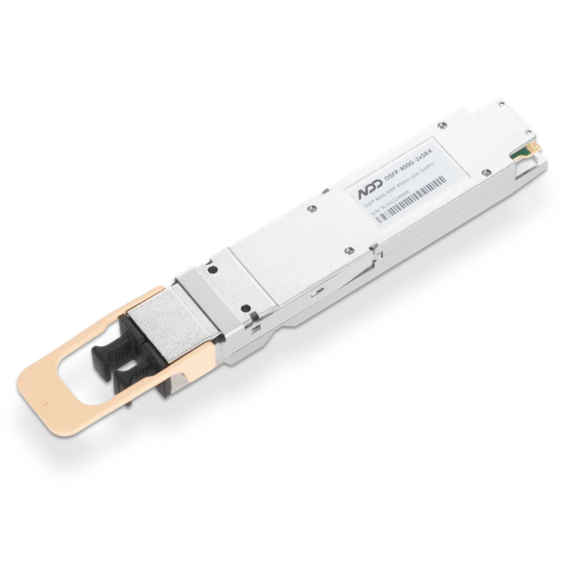 800GBASE-2xSR4 OSFP PAM4 850nm 50m MMF Module

 800GBASE-2xSR4 OSFP PAM4 850nm 50m MMF Module


