


Find the best fit for your network needs

share:
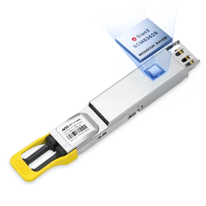
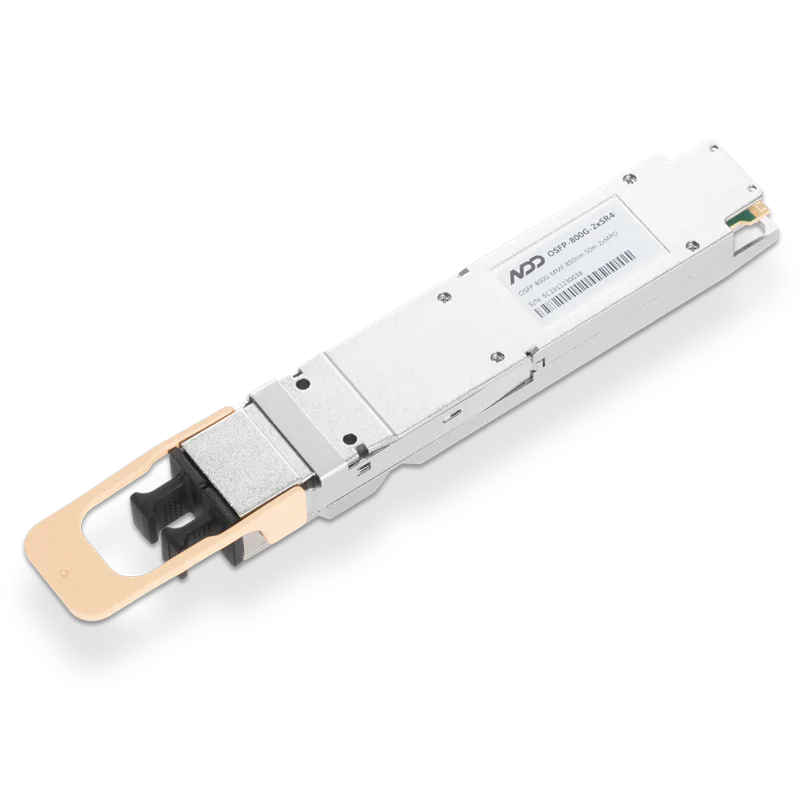 800GBASE-2xSR4 OSFP PAM4 850nm 50m MMF Module
Learn More
Popular
- 1High-Performance GPU Server Hardware Topology and Cluster Networking-2
- 2High-Performance GPU Server Hardware Topology and Cluster Networking-L40S
- 3AI Intelligent Computing Center Network Architecture Design Practice
- 4The Key Role of High-quality Optical Transceivers in AI Networks
- 5Common Problems While Using Optical Transceivers in AI Clusters