


Find the best fit for your network needs

share:
Copy Link
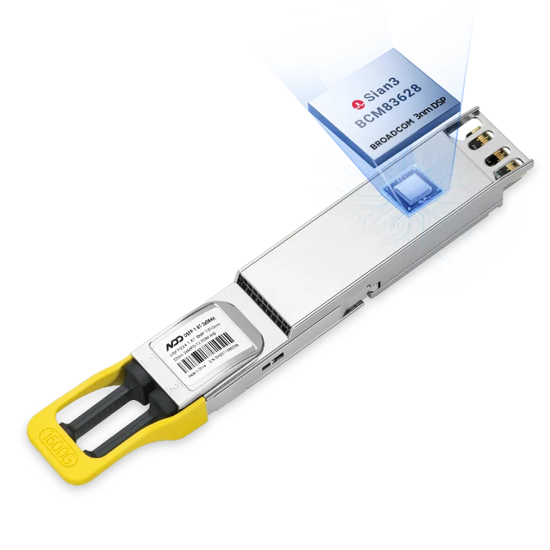
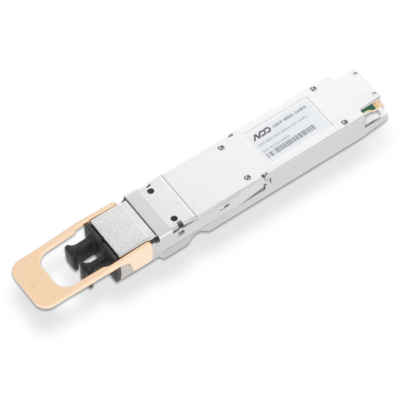 800GBASE-2xSR4 OSFP PAM4 850nm 50m MMF Module
Learn More
Let's Chat
United States
United Kingdom
Canada
Australia
France
Germany (Deutschland)
Spain (España)
Italy (Italia)
Netherlands
India
Brazil
Switzerland
Afghanistan
Albania
Algeria
American Samoa
Andorra
Angola
Anguilla
Antigua and Barbuda
Argentina
Armenia
Aruba
Austria
Azerbaijan
Bahamas
Bahrain
Bangladesh
Barbados
Belgium
Belize
Benin
Bermuda
Bhutan
Bolivia
Bosnia and Herzegovina
Botswana
British Indian Ocean Territory
Brunei Darussalam
Bulgaria
Burkina Faso
Cambodia
Cameroon
Cape Verde
Cayman Islands
Chad
Chile
China
Christmas Island
Cocos (Keeling) Islands
Colombia
Comoros
Cook Islands
Costa Rica
Cote D'Ivoire
Croatia
Cyprus
Czech Republic
Denmark
Djibouti
Dominica
Dominican Republic
Timor-Leste
Ecuador
Egypt
El Salvador
Equatorial Guinea
Eritrea
Estonia
Ethiopia
Falkland Islands (Malvinas)
Faroe Islands
Fiji
Finland
French Guiana
French Polynesia
French Southern Territories
Gabon
Gambia
Georgia
Ghana
Gibraltar
Greece
Greenland
Grenada
Guadeloupe
Guam
Guatemala
Guinea
Guinea-bissau
Guyana
Haiti
Heard and Mc Donald Islands
Honduras
Hong Kong, China
Hungary
Iceland
Indonesia
Ireland
Israel
Jamaica
Japan
Jordan
Kazakhstan
Kenya
Kiribati
Republic of Korea
Kuwait
Kyrgyzstan
Lao,P.D.R.L
Latvia
Lesotho
Liberia
Liechtenstein
Lithuania
Luxembourg
Macao, China
The Republic of North Macedonia
Madagascar
Malawi
Malaysia
Maldives
Mali
Malta
Marshall Islands
Martinique
Mauritania
Mauritius
Mayotte
Mexico (México)
Micronesia,F.S.O.M
Moldova
Monaco
Mongolia
Montserrat
Morocco
Mozambique
Myanmar
Namibia
Nauru
Nepal
New Caledonia
New Zealand
Niger
Nigeria
Niue
Norfolk Island
Northern Mariana Islands
Norway
Oman
Pakistan
Palau
Panama
Papua New Guinea
Paraguay
Peru
Philippines
Pitcairn
Poland
Portugal
Puerto Rico
Qatar
Reunion
Romania
Russian Federation (Россия)
Rwanda
Saint Kitts and Nevis
Saint Lucia
Saint Vincent and the Grenadines
Samoa
San Marino
Sao Tome and Principe
Saudi Arabia
Senegal
Seychelles
Sierra Leone
Singapore
Slovakia (Slovak Republic)
Slovenia
Solomon Islands
South Africa
South Georgia & T.S.S.I
Sri Lanka
St. Helena
St. Pierre and Miquelon
Suriname
Svalbard & J.M.I
Swaziland
Sweden
Taiwan, China
Tajikistan
Tanzania,U.R.O.T
Thailand
Togo
Tokelau
Tonga
Trinidad and Tobago
Tunisia
Turkey
Turkmenistan
Turks & Caicos Islands
Tuvalu
Uganda
Ukraine
United Arab Emirates
Uruguay
Uzbekistan
Vanuatu
Vatican City State (Holy See)
Vietnam
Virgin Islands (British)
Virgin Islands (U.S.)
Wallis and Futuna Islands
Western Sahara
Serbia
Zambia
Aland Islands
Palestinian Territory
Montenegro
Guernsey
Isle of Man
Jersey
Canary Islands
The Republic of Congo
St. Barthelemy
St. Martin
Bonaire
Curaçao
Sint-Maarten
Saba
Sint Eustatius
+1
I agree to NADDOD's Privacy Policy and Term of Use.
Submit
Find the ideal optical and connectivity solutions to elevate your network!
Shop now
United States
United Kingdom
Canada
Australia
France
Germany (Deutschland)
Spain (España)
Italy (Italia)
Netherlands
India
Brazil
Switzerland
Afghanistan
Albania
Algeria
American Samoa
Andorra
Angola
Anguilla
Antigua and Barbuda
Argentina
Armenia
Aruba
Austria
Azerbaijan
Bahamas
Bahrain
Bangladesh
Barbados
Belgium
Belize
Benin
Bermuda
Bhutan
Bolivia
Bosnia and Herzegovina
Botswana
British Indian Ocean Territory
Brunei Darussalam
Bulgaria
Burkina Faso
Cambodia
Cameroon
Cape Verde
Cayman Islands
Chad
Chile
China
Christmas Island
Cocos (Keeling) Islands
Colombia
Comoros
Cook Islands
Costa Rica
Cote D'Ivoire
Croatia
Cyprus
Czech Republic
Denmark
Djibouti
Dominica
Dominican Republic
Timor-Leste
Ecuador
Egypt
El Salvador
Equatorial Guinea
Eritrea
Estonia
Ethiopia
Falkland Islands (Malvinas)
Faroe Islands
Fiji
Finland
French Guiana
French Polynesia
French Southern Territories
Gabon
Gambia
Georgia
Ghana
Gibraltar
Greece
Greenland
Grenada
Guadeloupe
Guam
Guatemala
Guinea
Guinea-bissau
Guyana
Haiti
Heard and Mc Donald Islands
Honduras
Hong Kong, China
Hungary
Iceland
Indonesia
Ireland
Israel
Jamaica
Japan
Jordan
Kazakhstan
Kenya
Kiribati
Republic of Korea
Kuwait
Kyrgyzstan
Lao,P.D.R.L
Latvia
Lesotho
Liberia
Liechtenstein
Lithuania
Luxembourg
Macao, China
The Republic of North Macedonia
Madagascar
Malawi
Malaysia
Maldives
Mali
Malta
Marshall Islands
Martinique
Mauritania
Mauritius
Mayotte
Mexico (México)
Micronesia,F.S.O.M
Moldova
Monaco
Mongolia
Montserrat
Morocco
Mozambique
Myanmar
Namibia
Nauru
Nepal
New Caledonia
New Zealand
Niger
Nigeria
Niue
Norfolk Island
Northern Mariana Islands
Norway
Oman
Pakistan
Palau
Panama
Papua New Guinea
Paraguay
Peru
Philippines
Pitcairn
Poland
Portugal
Puerto Rico
Qatar
Reunion
Romania
Russian Federation (Россия)
Rwanda
Saint Kitts and Nevis
Saint Lucia
Saint Vincent and the Grenadines
Samoa
San Marino
Sao Tome and Principe
Saudi Arabia
Senegal
Seychelles
Sierra Leone
Singapore
Slovakia (Slovak Republic)
Slovenia
Solomon Islands
South Africa
South Georgia & T.S.S.I
Sri Lanka
St. Helena
St. Pierre and Miquelon
Suriname
Svalbard & J.M.I
Swaziland
Sweden
Taiwan, China
Tajikistan
Tanzania,U.R.O.T
Thailand
Togo
Tokelau
Tonga
Trinidad and Tobago
Tunisia
Turkey
Turkmenistan
Turks & Caicos Islands
Tuvalu
Uganda
Ukraine
United Arab Emirates
Uruguay
Uzbekistan
Vanuatu
Vatican City State (Holy See)
Vietnam
Virgin Islands (British)
Virgin Islands (U.S.)
Wallis and Futuna Islands
Western Sahara
Serbia
Zambia
Aland Islands
Palestinian Territory
Montenegro
Guernsey
Isle of Man
Jersey
Canary Islands
The Republic of Congo
St. Barthelemy
St. Martin
Bonaire
Curaçao
Sint-Maarten
Saba
Sint Eustatius
+1
I agree to NADDOD's Privacy Policy and Term of Use.
Submit