InfiniBand Network
RoCE Network
Comprehensive AI Network Architecture
Immersion Cooling Network
Let's Chat
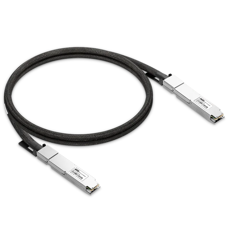
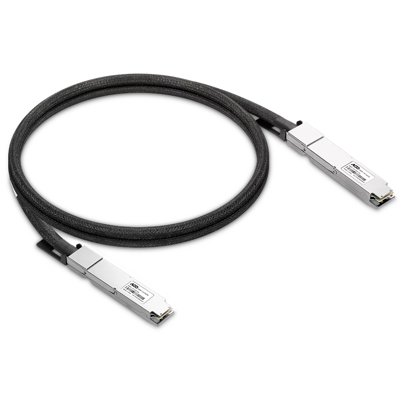
NVIDIA/Mellanox MCP4Y10-N001 Compatible DAC 1m (3ft) Twin-port 2x400Gb/s OSFP Finned Top to 2x400Gb/s OSFP Finned Top InfiniBand NDR Passive Copper Cable
US$ 139.00
NVIDIA/Mellanox MMA4Z00-NS Broadcom DSP & Broadcom VCSEL Compatible 800G 2xSR4/SR8 OSFP PAM4 850nm 50m DOM Two MPO-12/APC InfiniBand NDR Transceiver Module for MMF (Finned Top)
US$ 769.00
NVIDIA/Mellanox MMA4Z00-NS400 Broadcom DSP & Broadcom VCSEL Compatible 400G SR4 OSFP PAM4 850nm 50m DOM Single MPO-12/APC InfiniBand NDR Transceiver Module for MMF (Flat Top)
US$ 659.00
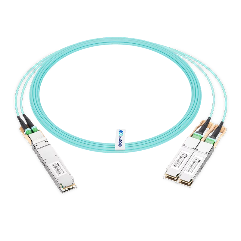
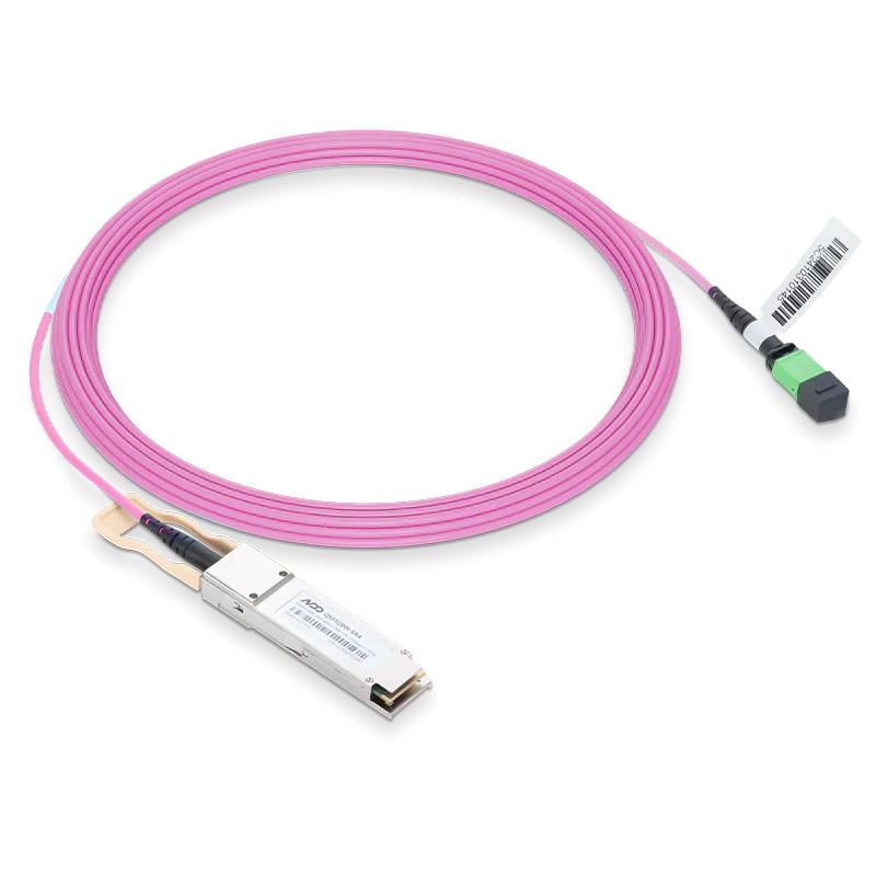
NVIDIA/Mellanox MFA7U10-H003 Compatible AOC 3m (10ft) 400Gb/s OSFP to 2x200Gb/s QSFP56 InfiniBand HDR Active Optical Splitter Cable (Finned Top, 850nm, MMF, LSZH)
US$ 928.00
NVIDIA/Mellanox MCP7Y00-N001 Compatible DAC 1m (3ft) Twin-port 2x400Gb/s OSFP Finned Top to 2x400Gb/s OSFP Flat Top InfiniBand NDR Passive Copper Splitter Cable
US$ 189.00
NVIDIA/Mellanox MMS4X50-NM Compatible 800G 2xFR4 OSFP PAM4 1310nm 2km DOM Two LC Duplex InfiniBand NDR Transceiver Module for SMF (Finned Top)
US$ 1399.00
NVIDIA/Mellanox MCX75310AAS-NEAT ConnectX®-7 InfiniBand & Ethernet Adapter Card, NDR 400Gb/s, Single-Port OSFP, PCIe 4.0/5.0 x 16, Tall Bracket
US$ 1499.00
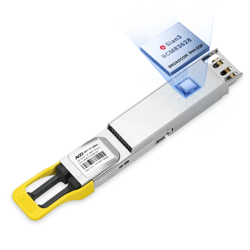
NVIDIA/Mellanox MMS4A00-XM/MMS4C10-XM (980-9IAH1-00XM00/980-9IAU0-00XM01) Compatible 1.6T 2xDR4/DR8 OSFP224 IHS/Closed Finned Top PAM4 Broadcom 3nm DSP (Sian3 | BCM83628) 1310nm 500m SMF DOM Dual MPO-12/APC InfiniBand XDR Transceiver Module for Quantum-X800 Air-Cooled Switches
US$ 1999.00
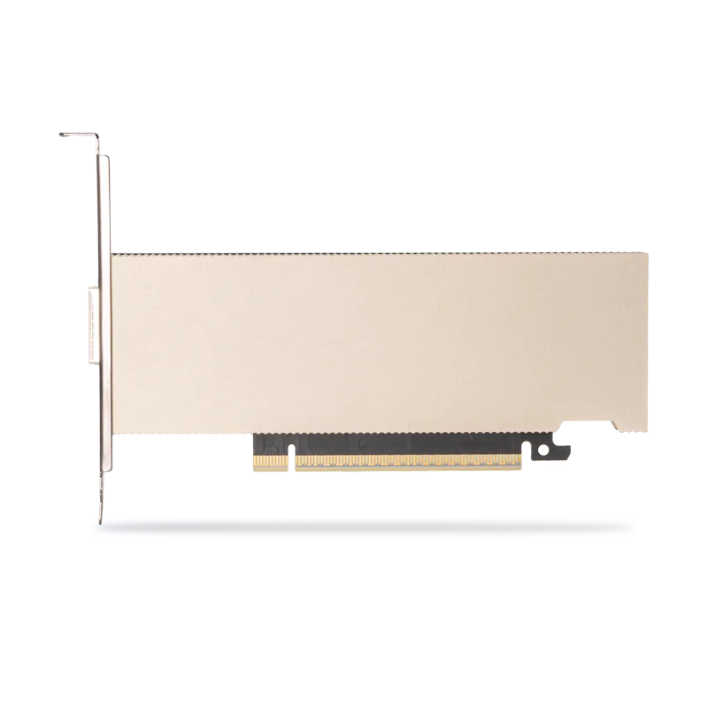
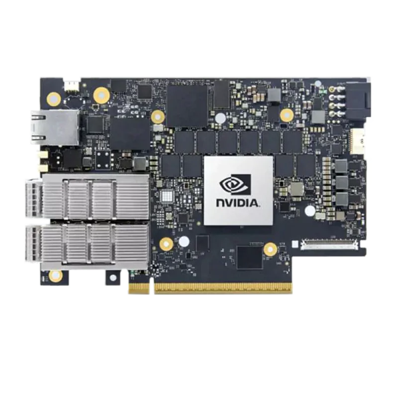
NVIDIA B3220 BlueField-3 DPU, P-Series FHHL, 200GbE (Default Mode)/NDR200 lB, Single-Slot Dual-port QSFP112, PCle Gen5.0 x16 with x16 PCle Extension Option, 16 Arm Cores, 32GB Onboard DDR, Integrated BMC, Crypto Disabled, Tall Bracket
US$ 3159.00
NVIDIA/Mellanox MFS1S90-H003E Compatible AOC 3m (10ft) 2x200G QSFP56 InfiniBand HDR to 2xQSFP56 InfiniBand HDR Active Optical Cross Connect Splitter H-Cable (850nm , MMF)
US$ 1079.00


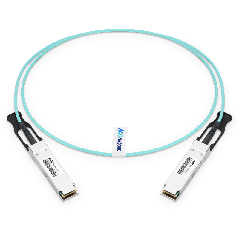


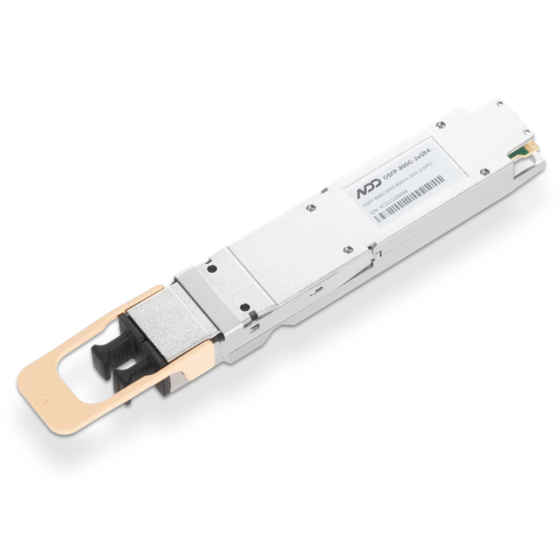 800GBASE-2xSR4 OSFP PAM4 850nm 50m MMF Module800GBASE-2xSR4 OSFP PAM4 850nm 50m MMF Module